
获取咨询
Liam@hengele.com Sale@hengele.com
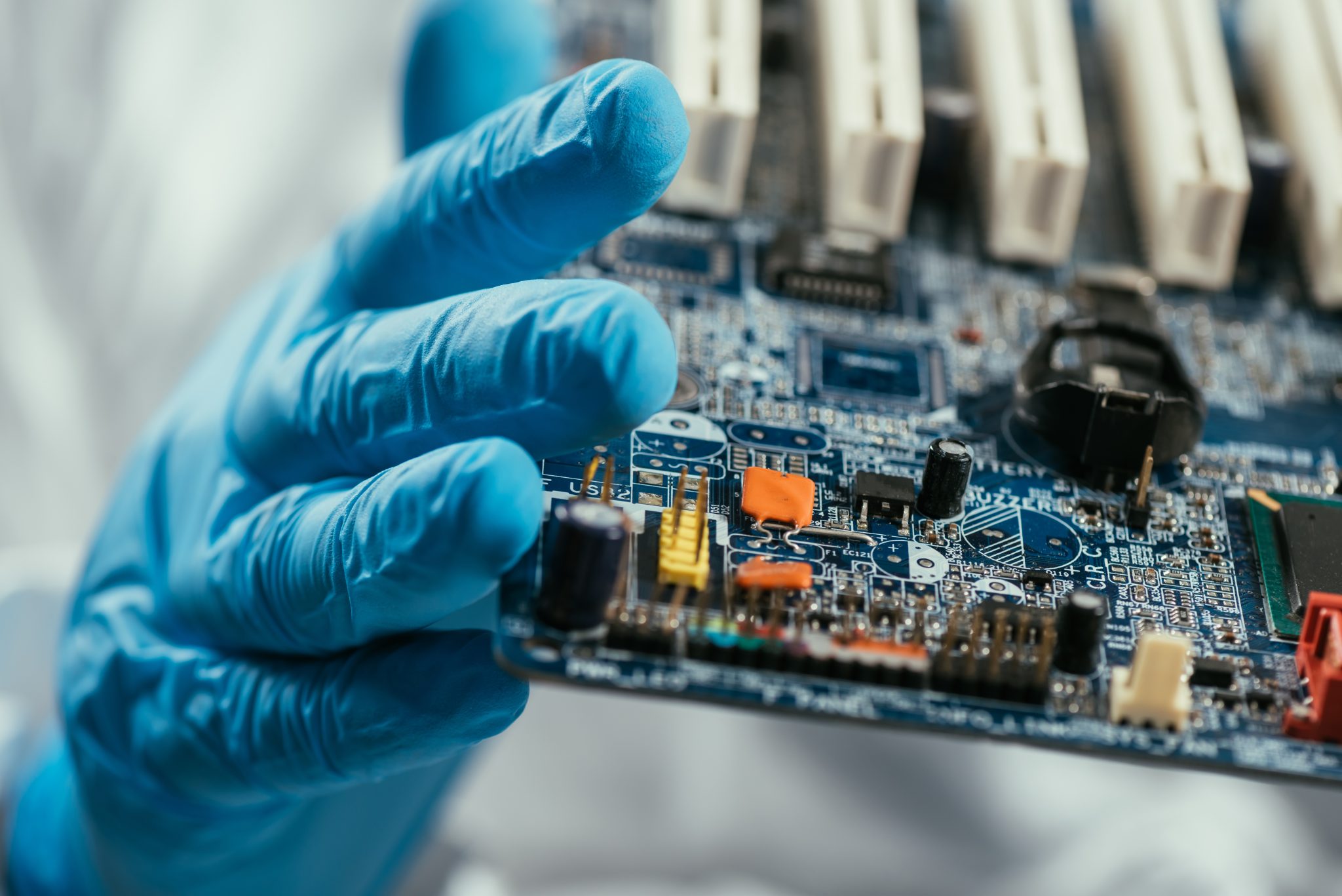
PCB组装工艺流程
The printed circuit board (PCB) is one of the core components of modern electronic products. Its main function is to ensure the stability and efficient operation of a circuit system by integrating key electronic components in an orderly and compact structure. For different types of products, PCBs often require specialized design to ensure that they meet strict technical standards for functionality, quality and durability.
Choosing a PCB manufacturer with proven technology and service is critical in the electronics manufacturing process. An experienced supplier not only improves product performance, but also helps customers control costs, shorten lead times, and streamline the entire process from design to mass production, including pre-consultation, prototyping, volume assembly, and logistics.
Hentech is committed to providing customers with one-stop PCB solutions. Headquartered in Shenzhen, China, we have been providing professional services to the North American market since 2018 for a wide range of industries including medical devices, communication systems, industrial applications and commercial electronics. With our advanced automated placement equipment and through-hole insertion process, we are capable of handling PCB assembly tasks of all levels of complexity, even complete machine integration production.
Hentech is your trusted partner in electronics manufacturing, helping you efficiently realize your products and drive your business forward.
Project initiation phase, communication, evaluation and quotation
The start-up phase of a PCB project, especially when developing a new product for the first time or working with a new manufacturer, is often full of challenges and uncertainty. We understand the importance of this phase and provide professional support to ensure that everything from communication to quotation is efficient and well organized.
◎ The working principle and key performance indicators of the product.
◎ Temperature, humidity, vibration and other factors affecting the application environment.
◎ Expected output demand and production technology requirements.
With this key information in hand, we will develop a detailed and competitive quotation for you. We will then proceed with the design of the necessary engineering documentation and move forward with the sampling and prototyping process, laying a solid foundation for subsequent volume production.
Our goal is to make every project clear, robust and trustworthy from the start.
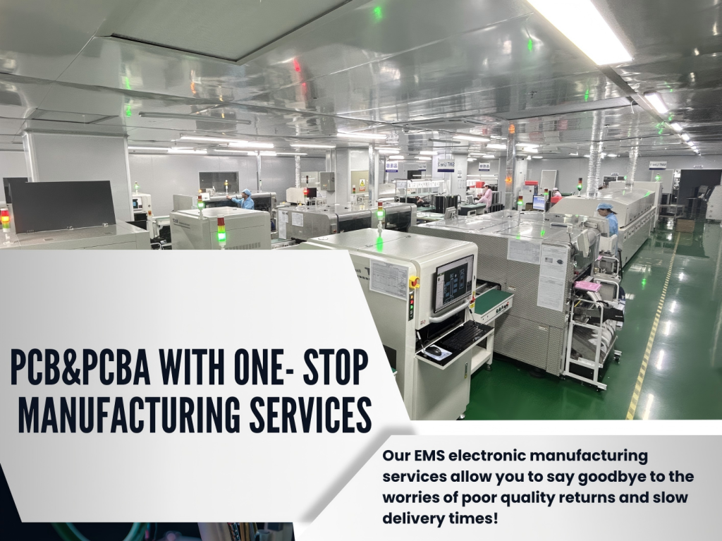
Our production site
Provide high-end SMT chip processing services, equipped with three automatic high-speed SMT chip production line, automatic board loading machine, automatic solder paste printing machine, SPI solder paste thickness detector, ten temperature reflow soldering, AOI optical inspection equipment, X-Ray inspection machine, automatic wave soldering, automatic three-proof paint spraying machine, etc., through the IS09001: 2015 quality management system, IATF16949 automotive electronics certification, ISO13485 medical device management system certification.
Analysis of the standard process of electronic assembly
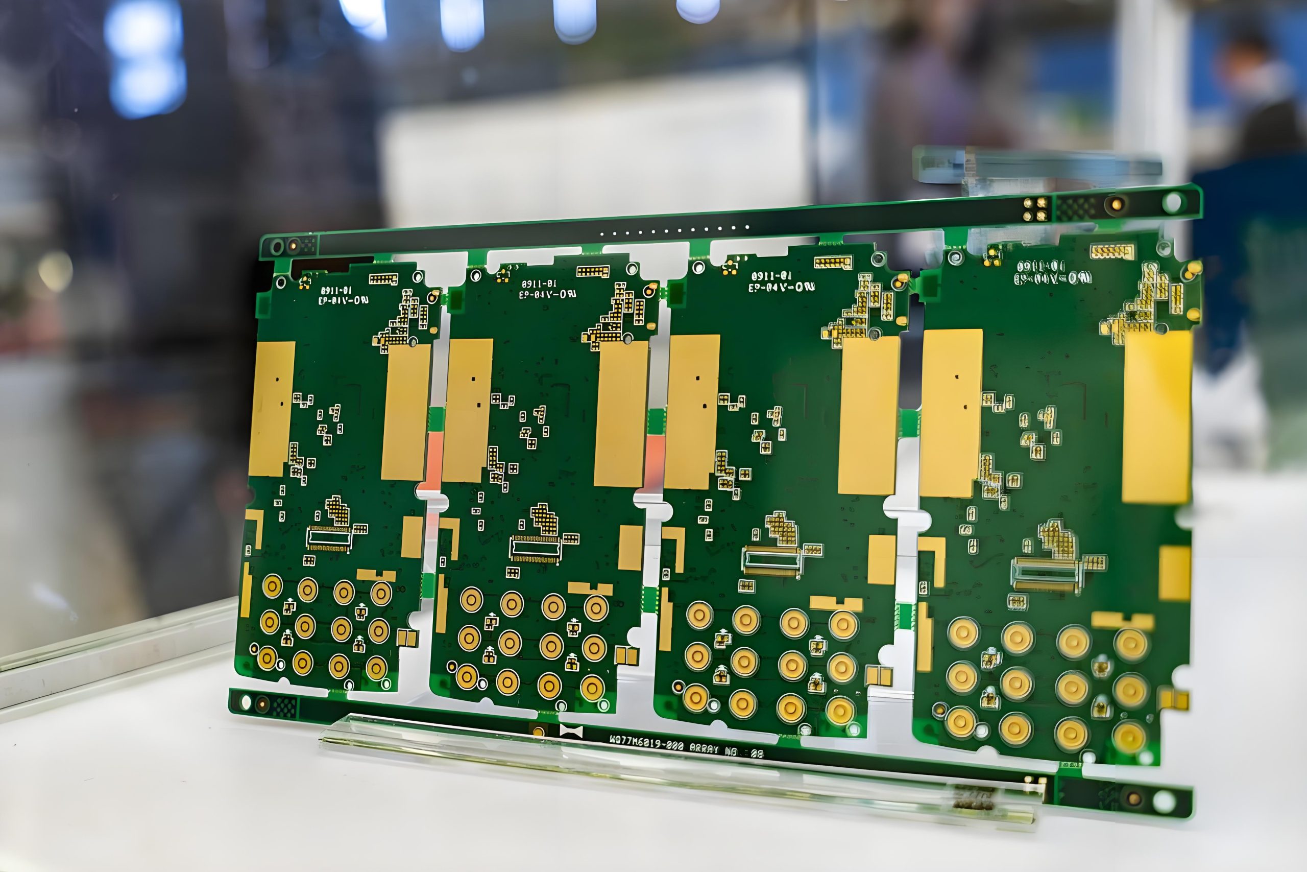
The assembly steps for each circuit board vary according to its design specifications. A typical PCB structure usually consists of a multilayer substrate, copper foils, dielectric layers, soldermasks, and silkscreen markings. Before assembly begins, we review the assembly instructions and design drawings provided by the customer to ensure that all processes meet precise manufacturing requirements. everything from communication to quotation is efficient and well organized.
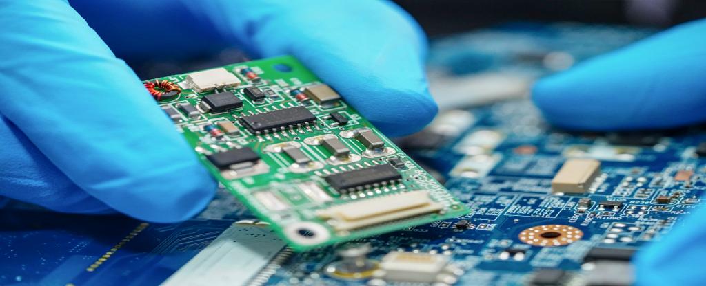
◎ Most high-density electronic products today utilize Surface Mount Technology (SMT), which offers the advantage of installing smaller, more compact components in a limited amount of space.
◎ SMT utilizes an automated placement machine to accurately locate the components, which are then securely soldered to the PCB surface through the reflow soldering process. This process not only improves assembly efficiency, but also reduces overall production costs.
◎ Through-hole technology is used in applications that require high mechanical strength, such as industrial, automotive or military equipment. The process consists of drilling holes in the circuit board, inserting components with pins and fixing them using wave soldering or hand soldering.
◎ This method, although more time-consuming, results in a more robust, tensile-strength soldered structure.
By combining SMT and THT processes, we are able to flexibly respond to the needs of a wide range of products and provide our customers with high-quality, reliable electronic assembly solutions.
Comprehensive quality testing guarantees the reliability of your products
During PCB assembly, we utilize an advanced automated process for solder coating to reduce potential manufacturing defects such as short circuits, bad solder joints, or warped pins. The automated process significantly improves consistency and yield, providing a strong guarantee of product performance.
To ensure that every board meets our stringent quality standards, our inspection team utilizes three-dimensional automated optical inspection (AOI) technology to perform a thorough visual inspection of components, accurately catching possible mounting deviations or soldering issues.
In addition, depending on lot size and the complexity of the board design, we perform functional testing and other electrical evaluations to identify problems such as incorrect component polarity, part damage, or misassembly. System-level testing also identifies detailed soldering defects, such as insufficient solder joints, solder vias, or bridges, to ensure that every product delivered will perform well in service and be reliable.
Quick Request a Quote Form
Ready to get started? Get in touch today to learn more about our surface mount circuit board assembly services and book a consultation at your convenience by filling out our request a quote form. If you don’t have design or Gerber files we’ll work with you to create a design. If you require a quick turnaround PCB quote or lead time, please let us know and we’ll work with you to accommodate your specific needs.

Sed ut perspiciatis unde omnis iste natus delavirot voluptatem accusantium doloremque laudanti totam aperiam inventore veritatis congueu. Olutpat elit nec nisi congue tristique eu at velit.
Hotline : (+62) 111 33 231
电话号码
+86 137 9821 9394
电子邮箱
Sale@hengele.com
Location
深圳市宝安区西乡街道臣田社区宝田二路2号臣田工业区28栋3层
Customer Service
Subscribe Newsletter
Sed ut perspiciatis unde omnis iste natus feria delavirot.
PCB layout and component setup preparation
The overall composition of a PCB depends on the project requirements. The substrate of the board is made up of multiple layers of material and is wired with copper foil. Before starting any component assembly, the assembler must review the design documents and evaluate any potential faults in the PCB that could affect performance.
How the unit is assembled depends on which of two mounting methods is used: surface mount or through-hole assembly.
PCB Assembly Process Overview: Surface Mount Assembly (SMT)
Today, most printed circuit boards are assembled using surface mount technology (SMT). Surface mount technology allows for smaller, more compact component packaging, and reduces production time and overall costs.
Hentech is proud to offer high quality PCBs at competitive prices.
Whether you’re looking for prototyping, low-volume trial production, or high-volume deliveries, our manufacturing partnerships provide the precision and flexibility to respond to your PCB requirements.
With a global manufacturing network, we are able to utilize a wide range of materials and advanced processes to produce complex multi-layer structures ranging from single-sided and double-sided boards to high-density interconnects (HDIs) and sequence building units (SBUs). Whether it’s a project with special requirements for mechanical and thermal properties, material types, or a design with high functional density, we offer reliable solutions.
Our resources allow for a seamless transition from rapid prototyping to mass production, with a range of layers from 1 to 64, ensuring high quality and efficient support at every stage of your project.
Choose the right PCB assembly technology for your project
In PCB assembly, choosing the right production process is critical to both product performance and cost control. Surface mount technology (SMT) offers higher production efficiencies and is particularly suited to smaller electronic products that require compact layouts. This technology is able to support smaller component arrangements and is the mainstream choice for modern commercial electronics manufacturing.
In contrast, through-hole assembly, while slightly slower in terms of production speed, offers significant advantages in terms of connection robustness and long-term reliability, and is particularly suitable for devices operating in extreme environments. For this reason, military, aerospace, and other sectors with stringent stability requirements often utilize the through-hole process.
Hentech offers both SMT and through-hole assembly capabilities. Based on your product requirements, budget, and operating environment, we will evaluate and recommend the most appropriate production method to help you realize your design in the most cost-effective way.
Quick Request a Quote Form
Ready to get started? Get in touch today to learn more about our surface mount circuit board assembly services and book a consultation at your convenience by filling out our request a quote form. If you don’t have design or Gerber files we’ll work with you to create a design. If you require a quick turnaround PCB quote or lead time, please let us know and we’ll work with you to accommodate your specific needs.
Sed ut perspiciatis unde omnis iste natus delavirot voluptatem accusantium doloremque laudanti totam aperiam inventore veritatis congueu. Olutpat elit nec nisi congue tristique eu at velit.
电话号码
+86 137 9821 9394
电子邮箱
Sale@hengele.com
Location
深圳市宝安区西乡街道臣田社区宝田二路2号臣田工业区28栋3层
Customer Service
Subscribe Newsletter
Sed ut perspiciatis unde omnis iste natus feria delavirot.